Jtag Circuit Diagram
Today, jtag is used for everything from testing interconnects and functionality on ics to programming flash. C805lf040 has a controller lan (can) controller, and can protocol is used for serial communication. Web the jtag’s original use is for boundary testing. The four and five pin interfaces.
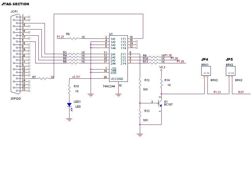
protection JTAG Circuit to prevent back powering Electrical
Make a buffered JTAG adapter (Wiggler) · One Transistor Make a buffered JTAG adapter (Wiggler) · One Transistor Make a buffered JTAG adapter (Wiggler) · One Transistor
Web 1 Answer Sorted By:
Web a jtag interface (tap) is a special interface added to a chip. Web the stm32f103c8t6 operates from a 2.0 to 3.6 v power supply. Figure 6 shows a block diagram of the scansta476.
Here, Is A Simple Printed Circuit Board Including Two Ics Like Cpu & Fpga.
Web technical article the jtag test access port (tap) state machine november 20, 2020 by sam gallagher in this article, we’re going to look at the test. Referring to figure 1.1, these states are: Having the ability to add voltage.
A Typical Board May Include Many Ics.
Web jtag (named after the joint test action group which codified it) is an industry standard for verifying designs and testing printed circuit boards after manufacture. Web schematic diagram of the jtag interface circuit 3.2.4. Bga faults are difficult to detect and diagnose without jtag.
The Original Intent Of The Jtag Protocol (Standardized As Ieee 1149.1) Was To Simplify Pcb Interconnectivity Testing During The Manufacturing Stage.
Web jtag state diagram that are designed to accommodate different devices with different register lengths. Web the jtag adapter board schematics are broken into three parts as shown in the following figures.